
Here is the second part of the RISC Processor Design. I have implemented this Processor as a part of my ASIC Design Lab project “Programmable Controller/Router and Peripheral Design with peripheral I/O multiplexing”. This project focuses of peripheral multiplexing to the GPIO pins of the processor in runtime. An example case will be a Pulse Width Modulated wave switching between any I/O pins during processor execution or an UART Transmitter pin routed to a pin based on board design without the need of external multiplexers.
The processor can access the peripherals via register write instructions. Similar to register file, the peripherals support two data reads and one data write simultaneously. Since I have used custom instructions, a custom Instruction Set Architecture (ISA) is also designed.
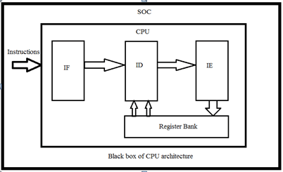
BLOCK DIAGRAM:

16-bit Instruction Format :
1. Register Instruction:
|
OPCODE [15:12]
|
DEST[11:8]
|
SRC_1 [7:4]
|
SRC_2 [3:0]
|
2. Immediate Instruction:
|
OPCODE [15:12]
|
DEST[11:8]
|
Immediate [7:0]
|
INSTRUCTION SET:
|
INSTRUCTION
|
OPCODE
|
INSTRUCTION
|
OPCODE
|
|
|
NOP
|
0000
|
NOT
|
0111
|
|
|
ADD
|
0001
|
MOV
|
1000
|
|
|
ADDI
|
0010
|
MVI
|
1001
|
|
|
SUB
|
0011
|
BC
|
1010
|
|
|
SUBI
|
0100
|
BS
|
1011
|
|
|
AND
|
0101
|
HLT
|
1111
|
|
|
OR
|
0110
|
REGISTER BANK:
The instructions that are supported by the CPU are mainly register instructions (R-type) and hence the register bank plays an important role in the execution of the instructions. There are a total of 16 registers available in the CPU all of which are 8 bits. The CPU registers (r0-r7) and peripheral registers share a common address space. Peripheral Address decoding is taken care by the peripherals themselves.

CPU SYNTHESIS (Synopsys Design Vision):
CPU module is synthesized and optimised in Synopsys design vision. The compiled schematic view is given below.

CPU VERIFICATION:

UART VERIFICATION:

TIMER VERIFICATION:

More details about individual modules will be discussed in future.
Author Profile
Latest entries
 ElectronicsMarch 3, 2019Sipeed Maix Bit, a 64-bit dual core RISC-V AI development board
 ElectronicsFebruary 18, 2017Building a 49cc Street Legal Motorized Bicycle
 ElectronicsDecember 28, 2016Programming STM32 ARM microcontrollers in Arch Linux
 ElectronicsMay 17, 2016ESP8266 – WiFi + Speech Controlled Hexapod Robot


